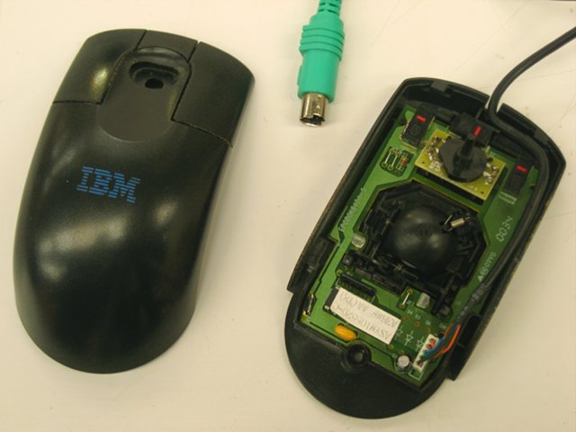
souris IBM MO09K
model : MO09K
P/N 28L1867
S/N 23-016694
This device complies with Canada ICES-003, Class B
US Pat No : 5 557 450
Germany Pat No : G9317838 7
Made in China
matériau ABS (indiqué en clair >ABS<)
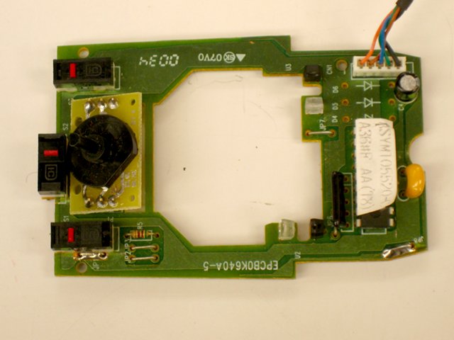
EPCBOK640A-5
Circuit double face avec composants mixtes CMS et classiques.
 photos en haute définition (17,1 MO)
circuit et composants
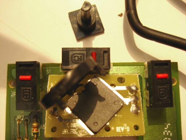
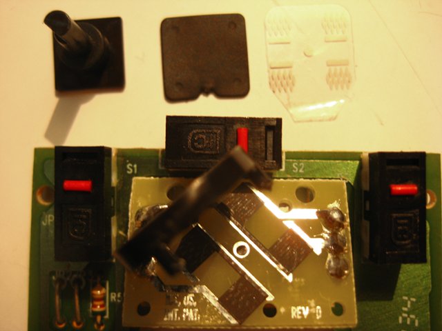
Face supérieure :
S1, S2, S3: micro-switch 1A, 125 VAC marque : IC ? (il y a un logo dessus)
PR1: resistive array ? marquage A5J103
R5 : R, 4 bandes, vert/marron/marron/doré, 510 Ohms +- 5%
Y1 : crystal, marquage A8.00 ??
C4 : condensateur électrochimique, 16 VDC, 47 µF
connecteur du cable PS/2 : 5 connections
LED infrarouges (x2) 2 pattes
phototransistors (x2) 3 pattes
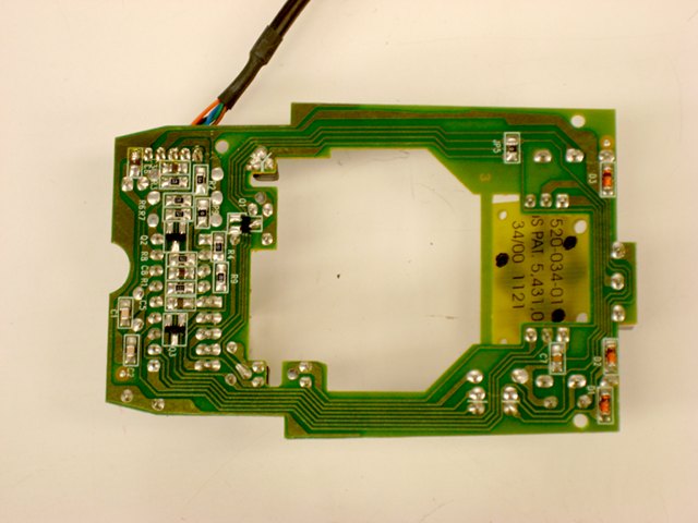
Sur l'autre face : composants CMS
diodes, transistors (?), C, R
Puce ASYM105520-C A36#F AA(T8) inscrit sur l'étiquette collée dessus.
sur la puce :
EICI132700
F 0031 (probablement la date de fabrication 31e semaine de 2000)
MC01 NF172 GV8
pas de marque visible, aucun datasheet ni info disponibles.
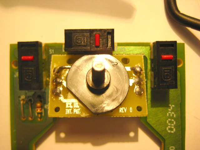
Au verso du Joystick une inscription :
520-034-01
US PAT. 5431064
34/00 1121
Le brevet déposé pour le joystick :
«
A pressure sensitive transducer array in which a plurality of transducers are connected in series and in parallel with one another. In one embodiment, a resistive layer is formed from carbon or silver ink on a polyester film. A plurality of conductive shunt elements having greater conductivity than the resistive layer is formed on a second polyester film. The films are placed adjacent to one another with the shunt elements contacting the resistive layer. Voltage is applied across the resistive layer and pressure is applied thereto. As the pressure increases, the number of current paths set up through contact points on the shunt elements increase thereby decreasing the resistance across the resistive layer and increasing current flow. In another embodiment a plurality of plate elements are contained in a plane on one side of a dielectric layer. A plurality of plate elements are contained in a plane on the other side of the dielectric layer. As the layer is pushed together responsive to force applied, total capacitance as measured across the planes of plate elements varies. »
On découvre 4 zones de détection, un filtre en polyester et une fine couche de carbone.
datasheets
/
ressources
/
